panelarrow

555 timer motor controller

Description.
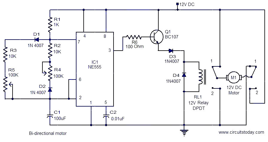
This is a simple and easy to construct circuit that can be used to provide a bidirectional drive to a DC motor. The circuit operation is straight forward. Output of an astable mutivibrator based on IC1 (NE555) is used to control the relay RL1 driving the motor. The motor is connected between the two poles of the relay contacts. The relay contacts are so wired as to reverse the DC supply to the motor when the contacts changeover.
The astable multivibrator produces a square wave at the output with its high time given by 0.69(R1+R3+R5)C1 and low time given by 0.69(R1+R2+R4)C1.The high and low times can be varied by varying potentiometers R4 and R5.For the given values the high and low times can be adjusted between 1S and 8S separately. When the IC1 output is low, the relay is de energised and the relay contacts are in position 1-1 with the result that A terminal of the motor is positive and motor runs in one direction. The IC1 output is high the relay is energised and the contacts changeover to position 2-2.Now the terminal B of the motor becomes positive and motor runs in the opposite direction. The transistor Q1 is used to drive the relay according to the output from IC1.The diode D4 acts as freewheeling diode.
Circuit diagram with Parts list.
bi-directional-motor


Notes.
  • Assemble the circuit on a good quality PCB.
  • The circuit can be powered from a 12V DC power supply.
  • The IC1 must be mounted on a holder.
  • The capacitor C1 must be rated at least 15V.
  • The relay RL1 can be a 12V DPDT relay.

Adjustable 10 minutes timer schematic

The 555 adjustable timer circuit starts timing when switched on. The green LED lights to show that timing is in progress. When the time period is over the green LED turns OFF, the red LED turns ON and the beeper sounds. The time period is set by adjusting the variable resistor. It can be adjusted from 1 to 10 minutes (approximately) with the parts shown in the diagram. You can mark the times on a scale drawn on the box.

Please note that the range of time periods is only approximate. With perfect components the maximum time period should be 4½ minutes, but this is typically extended to about 10 minutes because the 220µF timing capacitor slowly leaks charge. This is a problem with all electrolytic capacitors, but some leak more than others. In addition the actual value of electrolytic capacitors can vary by as much as ±30% of their rated value.

Adjustable 10 minutes timer schematic

adjustable timer schematic

1500 WATT AMPLIFIER
Circuit Power Amplifier has a power output of up to 1500W RMS power amplifier circuit is often used to power sound systems keperlun for outdor. In the final image can be seen a series of power amplifiers using 10 sets of power transistors for the ending.

This power amplifier circuit using a transistor amplifier from the front, signal splitter, driver and power amplifier. Current consumption required is quite large power amplifier that is 15-20 A 1500W power amplifier circuits for this. Supply voltage needed by the power of this amplifier is the optimal working order symmetrical 130VDC (130VDC-130VDC ground). 1500W amplifier circuit below is a picture series of mono, stereo if you want to make it necessary to make two copies of the circuit. For more details can be viewed directly image the following 1500W power amplifier circuit.
The series of High Power Amplifier 1500W With Transistor

400W AMPLIFIER WITH MOSFET

400W AMPLIFIER WITH MOSFET
Power amp 400W IRFP448 Circuit
Amplifier circuit today,We would like to show you for the MOSFET 400 watt amplifier is amplifier on my kW shares the same circuit and basic PCB layout.
  The only real difference is the number of output devices to the device.
  We have using The IRFP448 design while the MOSFET amplifier 14 O / P devices.
  These amplifiers can be used for virtually any application that requires high performance, low use Noise, distortion and excellent sound quality. Examples would be subwoofer amplifier should FOH stage
  Amplifiers, surround a canal a very powerful sound amplifier, etc.
  The 400W MOSFET-amplifier has four key stages of amplification. We are looking to start any   Phase appropriate detail.
The bias and buffer stage
  As the name suggests All Q ,C and ZD the Bias and buffer phases. Its main goal is to provide a stable MOSFET Gates  and offset voltage and the voltage buffer amplifier stage of the High Resource capacity. What would have without the phase response and the effect
  Slew rate is indeed very bad. The flip side of the coin is not the extra step
  Introduction of an additional dominant pole in the amplifier feedback loop.
400W MOSFET PCBhttps://blogger.googleusercontent.com/img/b/R29vZ2xl/AVvXsEgJ9H10xzHB-1e-eOl7vZNrNBbzEa5lquMffaukFHEwxi1QZ0l3V8DmTYCpbxO6zIjiv3IkOwMGF0vID0BrFKCyIwLek-C-XriyQYOsKRwNk6Z3ZBsVUESjwTNTP8yDu-za-cLaxaNPuh4/s1600/1545295N3-0.png

2000W AUDIO BOOSTER AMPLIFIER


 2000W AUDIO BOOSTER AMPLIFIER
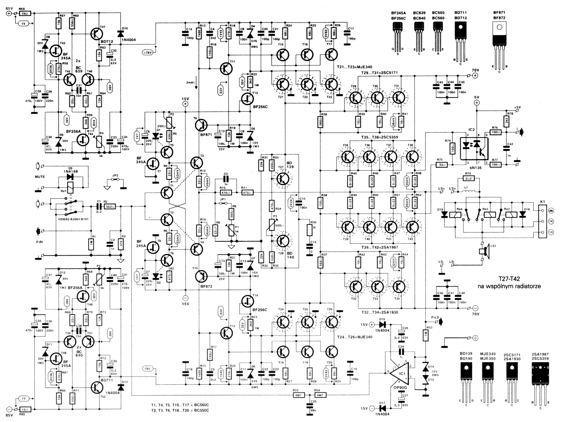
This is linear power amplifier 2000 Watt which need advance knowledge in electronics since the schematic diagram is very complex for hand made circuit. I think you have to re-design the schematic diagram using circuit diagram software designer such as diptrace, eagle, expresspcb ect. Or just order the PCB online, they will be glad to make the PCB for you.

This kind of power amplifier circuit need high power consumption, so you need to build the power supply carefully. It need dual polarity power supply (+85, 0, -85) and of course with high DC current of about 20A.
Just need to think again if you want to build this kind of power amplifier 2000 Watt. :)

Power Amplifier 2000 Watt was last modified: October 19th, 2015 by circuit diagram
electronic circuit

This is incredible 1000W Power Amplifier

This is incredible 1000W Power Amplifier

This is an audio amplifier circuit provides power to 1000 watts Blazer. This interesting routes under a lot of good and lively treble.
Importantly, you should choose the power source, which has been quite high voltage class GND-70V 70Vdc 10A is the current low level
The transistors are 2SC3858 (NPN) and 2SA1494 (PNP) and the bandwidth characteristic of high, excellent area of ​​safe operation, high linearity and high gain. 2SC5200 driver transistors (NPN) and 2SA1943 (PNP). All devices are rated at 230 V, with the power transistors has a dissipation of 150 W and the drivers are 50W.
This circuit describes a process amplifier, power supply and the tests that are inherently dangerous. Nothing described in this article should not even be considered unless a wealth of experience, we know exactly what you are doing and are willing to assume full responsibility for 100% of what you do. There are design issues that may require analysis, fault detection and / or modification.

Popular Posts

Recent Posts

Pages

Advertise

Copyright © next innovation